


Address:Building 10, Baijiahui Innovation Community, Xuanwu District, Nanjing, Jiangsu, China


PTFE-NZ
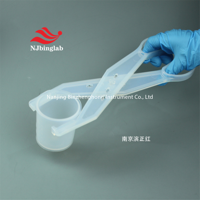
NJbinglab
PTFE
Isotope Industry, Semiconductor Industry
100mm/150mm/200mm/250mm/300mm
-200℃~+250℃
Corrosion Resistance
White opaque
Molded
1pc
7 Working Day
LOGO, Packaging, Pattern


Product Description
Product Overview: PTFE Tweezer
Crafted from high-purity Polytetrafluoroethylene (PTFE), this specialty tweezer represents a pinnacle of performance for demanding laboratory and industrial applications. Its inherent material properties offer unparalleled advantages in environments where contamination, corrosion, or interference are critical concerns.
PTFE Material Advantages:
PTFE is renowned for its exceptional chemical inertness, capable of resisting virtually all aggressive solvents, acids, alkalis, and bases. This ensures the tweezer will not corrode or degrade when handling harsh substances. Furthermore, PTFE is inherently hydrophobic and non-sticky, preventing samples from adhering to the tips. Its excellent non-conductive and low dielectric constant properties make it ideal for sensitive electronic work. Notably, PTFE operates effectively across a wide temperature range from -200°C to +260°C. Most importantly, as a fluoropolymer, it is biologically inert and exhibits extremely low levels of extractables and leachables, minimizing the risk of sample contamination.
Key Features & Functions:
* Ultra-Clean & Non-Contaminating: Perfect for handling sensitive samples in fields like cell culture, semiconductor processing, and analytical chemistry.
* Universal Chemical Resistance: Safely manipulates items exposed to corrosive chemicals without risk of tool failure or particle generation.
* Non-Marring & Anti-Static: Soft yet durable tips prevent damage or scratching of delicate surfaces (e.g., silicon wafers, optical components) and mitigate static build-up.
* Heat & Cold Resistant:Functions reliably in ovens, freezers, and during sterilization processes (where autoclave compatibility is specified).
* Non-Magnetic & Electrically Insulating:Essential for handling components in electronics, microscopy, and forensic analysis.
Typical Applications:
* Electronics & Semiconductor: Handling wafers, chips, and fragile SMD components.
* Life Sciences & Medical: Aseptic manipulation in cell biology, histology, and IVF procedures.
* Analytical Labs: Sample handling for HPLC, IC, and mass spectrometry; weighing procedures in analytical balances.
* Chemical Processing: Manipulating crystals, filters, or parts in corrosive environments.
* General Precision Handling: Ideal for cleanrooms, optical labs, and any scenario where metal tweezers pose a risk of contamination, damage, or interference.
In summary, the PTFE tweezer is an indispensable tool where material purity, chemical stability, and sample integrity are paramount, offering a reliable and contamination-free solution for precision manipulation.