Leave A Message
If you are interested in our products and want to know more details,please leave a message here,we will reply you as soon as we can.

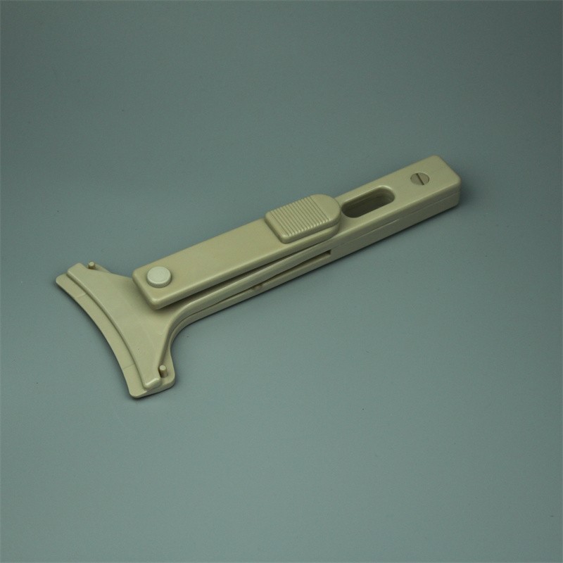
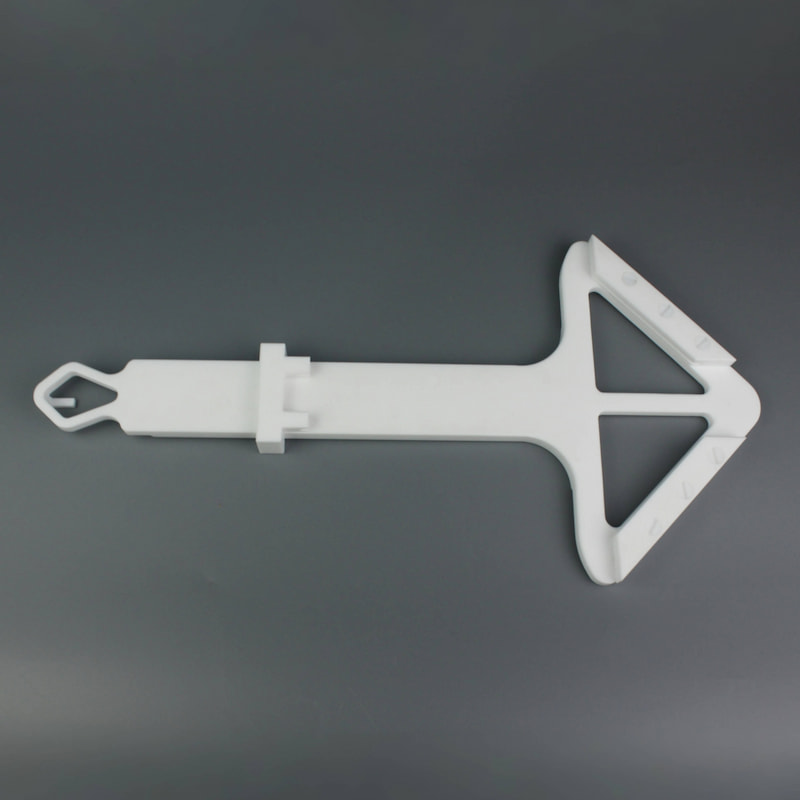
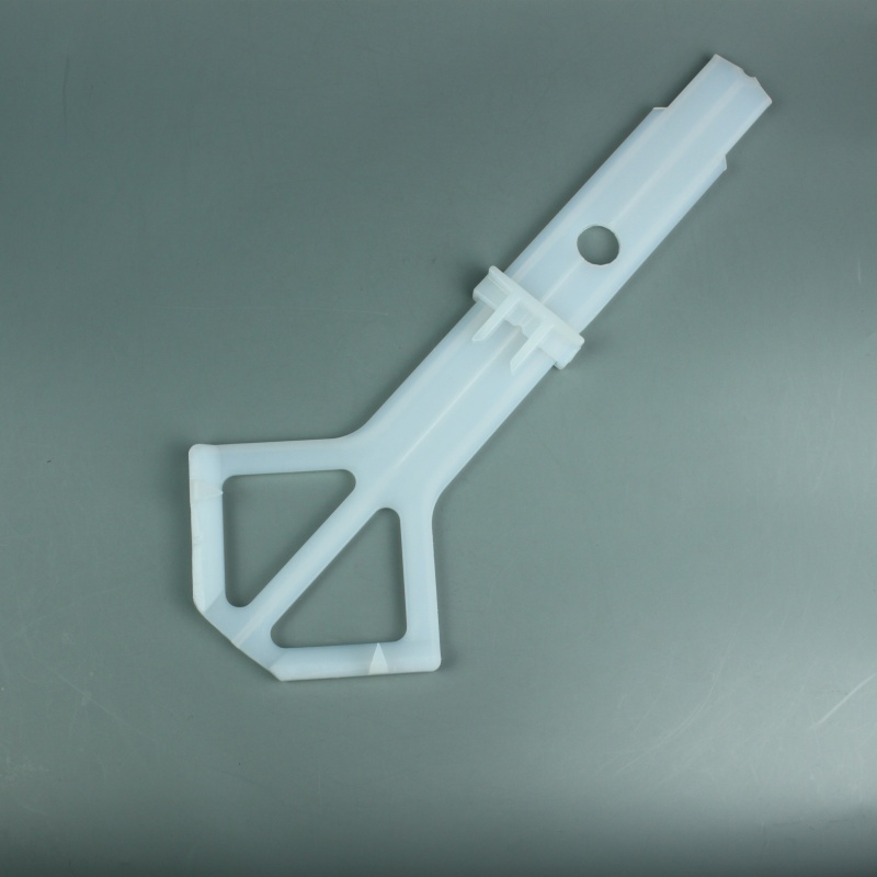
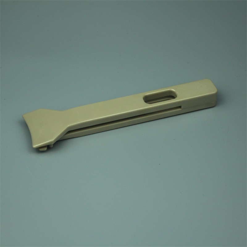
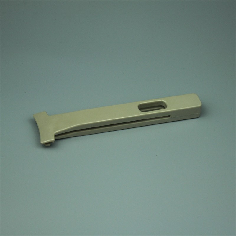
Precision Individual Handling: Specifically engineered for the safe pick-and-place of single wafers, preventing cross-contamination and surface damage.
Superior Mechanical Strength: Made from high-performance PEEK, providing the rigidity and "spring-back" memory required for consistent gripping force.
High-Heat Resilience: Capable of handling wafers directly from high-temperature processes (up to 260°C) without softening or deforming.
Non-Marring Contact: The smooth PEEK tips are designed to grip wafers by the edges or underside without scratching sensitive layers or leaving metallic traces.
Ergonomic Slide-Lock Design: Features a built-in sliding mechanism (only for 12") to lock the gripper in place, ensuring a fatigue-free and secure hold during transport.
Brand :
NJbinglabItem No :
PEEK-JYJ-12material :
PEEKSpecification :
12" waferThe PEEK Wafer Gripper is a specialized manual handling tool designed for the meticulous transfer of individual silicon wafers, compound semiconductors, and glass substrates. While vacuum wands can fail and traditional metal tweezers risk scratching, these PEEK grippers offer a perfect balance of structural hardness and surface gentleness. The material’s natural resistance to wear ensures that no particles are generated during the gripping action, maintaining the integrity of Class 1 cleanroom environments. Its robust construction makes it an indispensable tool for engineers performing manual inspections or loading wafers into specialized R&D equipment.
PEEK/PTFE Wafer Baskets: The ideal tool for loading individual wafers into cleaning baskets or retrieving them after a batch cycle.
PFA/PTFE Chemical Tanks: Allows for the manual "dipping" of single wafers into etchants while keeping the operator’s hands at a safe distance.
Semiconductor R&D: Manual handling of experimental wafers during layer deposition or lithography testing.
Failure Analysis: Precise extraction of individual die or wafer fragments for destructive and non-destructive testing.
MEMS & Nanotechnology: Handling of delicate micro-mechanical structures where vacuum wands might cause structural collapse.
Photovoltaic (Solar) Research: Sorting and inspecting high-efficiency silicon cells during the manufacturing process.
Leave A Message