Leave A Message
If you are interested in our products and want to know more details,please leave a message here,we will reply you as soon as we can.

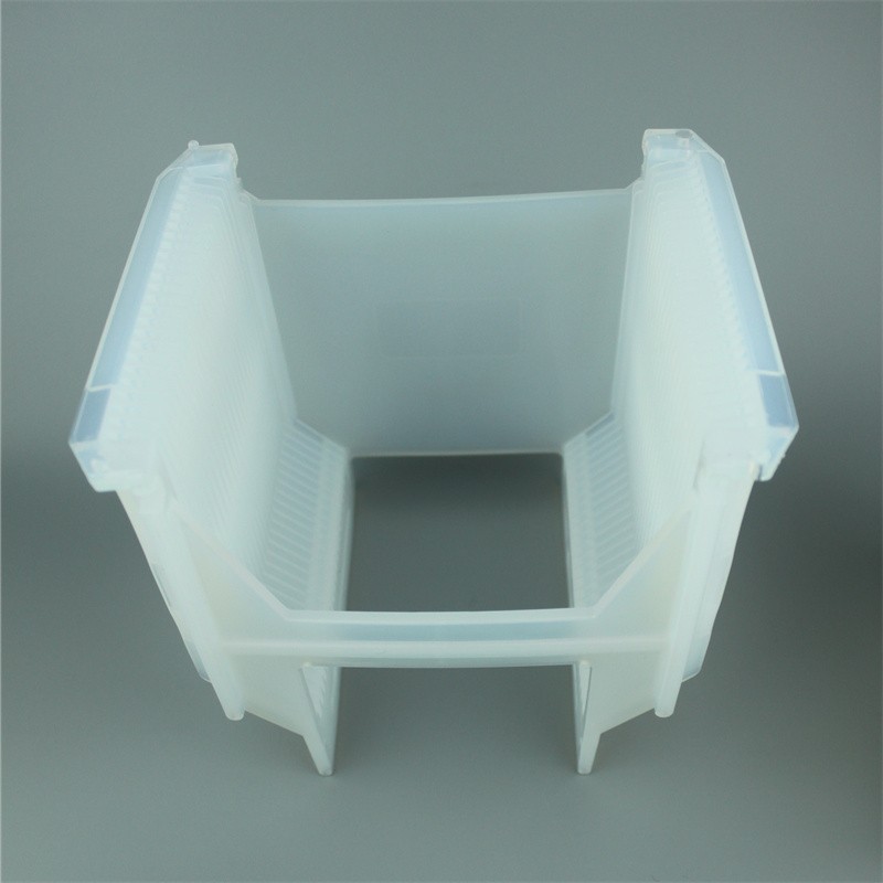
Semiconductor Purity: Fabricated from high-purity PFA to eliminate metal ion leaching and particle shedding.
Thermal Endurance: Engineered to withstand aggressive chemical baths at temperatures up to +260°C.
Universal Resistance: Fully inert to concentrated HF, H2SO4, and ultra-pure etching solutions.
Precision Geometry: Designed with specialized slots for maximum fluid circulation and secure wafer/substrate support.
Ergonomic Handling: Compatible with interchangeable PFA handles for safe, contamination-free transport in cleanrooms.
Brand :
NJbinglabItem No :
PFA-HL-6-25smaterial :
PFASpecification :
64 inches, 25 slotsThe PFA Cassette system is the gold standard for wafer and substrate processing in ultra-clean environments. Its robust, open-frame design ensures uniform exposure to process chemicals during cleaning, etching, and rinsing cycles. To ensure a fully integrated workflow, we provide matching Y-Type and M-Type PFA Handles. These handles are designed to snap securely onto the cassette, providing technicians with a safe, heat-resistant, and chemically inert grip to move high-value materials between acid baths and rinsing stations.
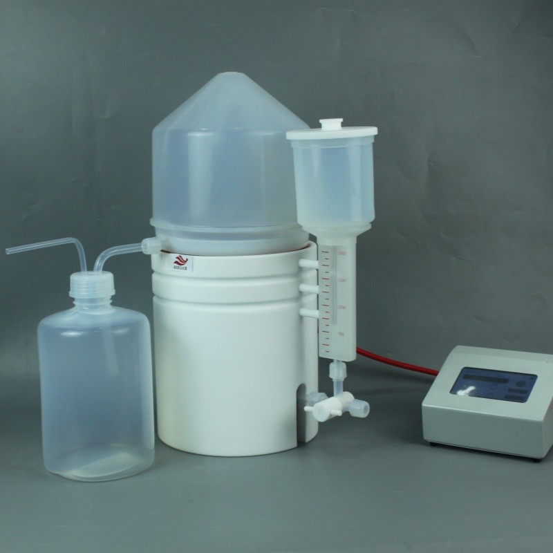
PFA Cleaning Tank: The cassette and handle are perfectly sized for batch submersion in our large-capacity PFA tanks.
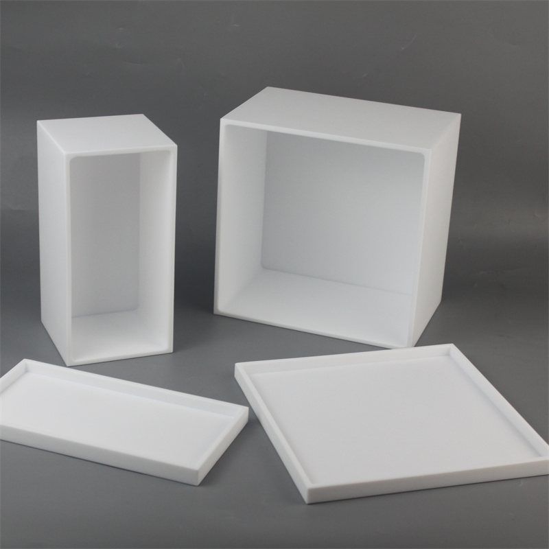
PFA Trays: Used as a secondary containment area for the cassette and handle post-processing to prevent floor or benchtop contamination.
PFA Fittings & Tubing: Integrated into the rinsing systems where the cassette-loaded wafers are cleaned with ultra-pure water.
Semiconductor Fabrication: Processing of 2", 4", 6", or 8" silicon wafers through harsh chemical etching cycles.
Photovoltaics (Solar): Handling of silicon substrates during surface texturing and doping preparations.
Optoelectronics: Cleaning of high-purity lenses and glass substrates for precision coating.
Advanced Materials: Batch decontamination of sensitive components in ultra-clean research environments.
Leave A Message