Leave A Message
If you are interested in our products and want to know more details,please leave a message here,we will reply you as soon as we can.

Brand :
NJbinglabItem No :
PTFE-GPHmaterial :
PTFESpecification :
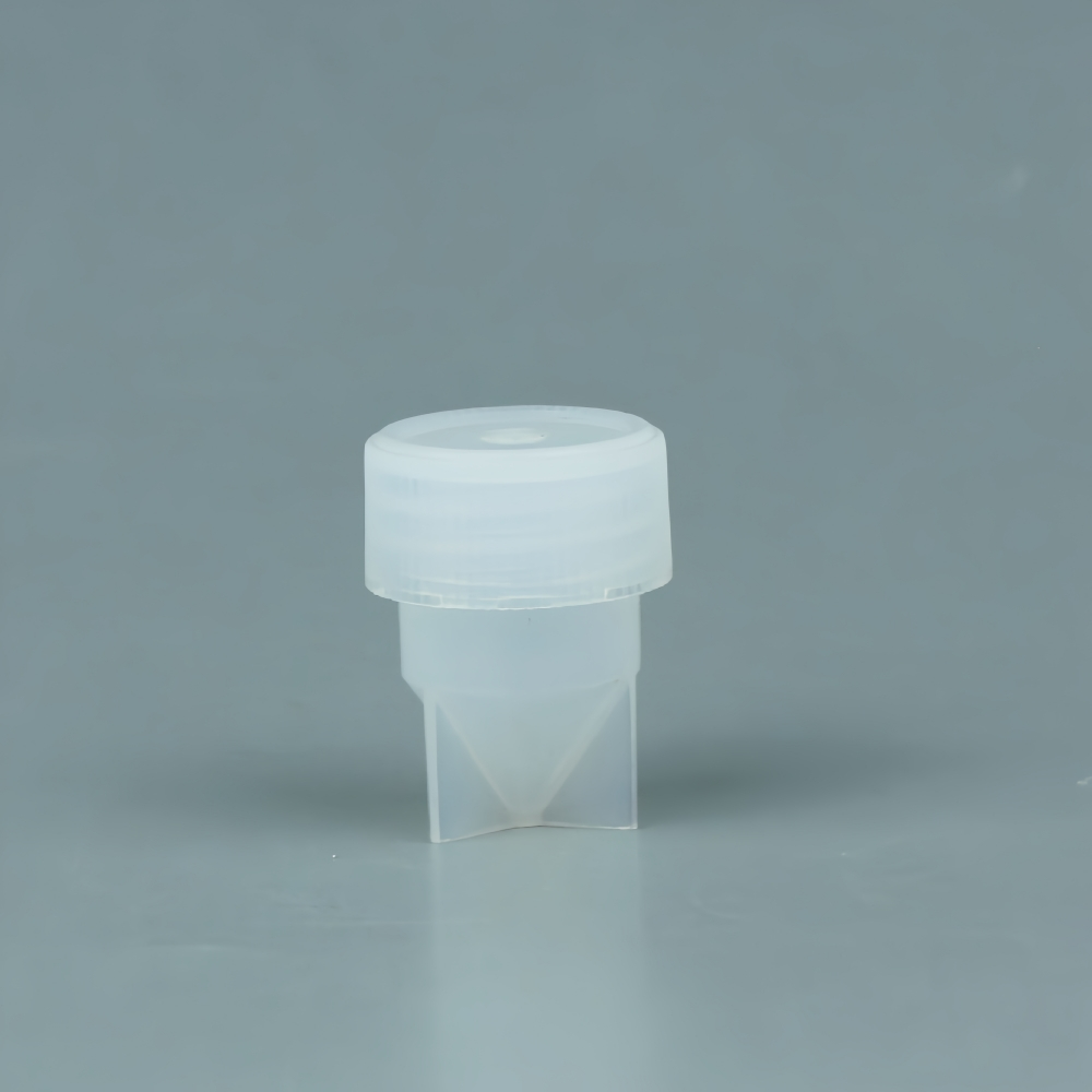
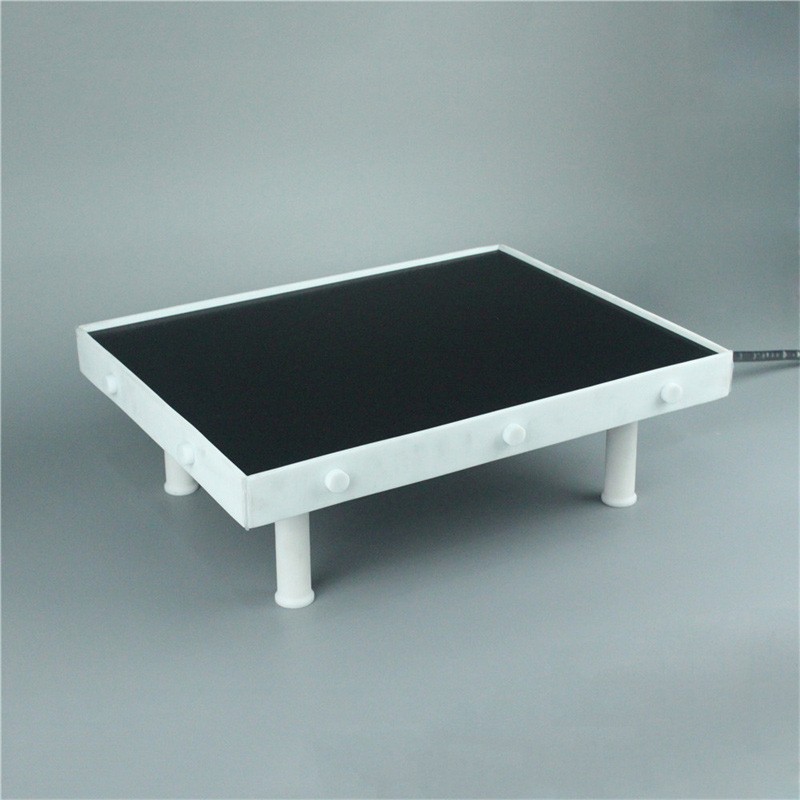
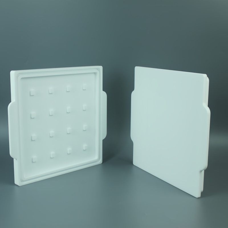
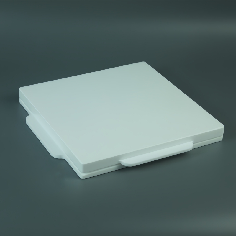
25*25*3mmThe PTFE Square Silicon Wafer Box (25×25×3 mm) is a precision-engineered storage and handling solution designed for small-format silicon wafers and delicate substrates. Manufactured from high-purity PTFE, this wafer box ensures a contamination-free environment, making it ideal for semiconductor processing, chemical cleaning, and ultra-trace analysis applications.
Its compact square design allows efficient organization and safe transport of wafers while maintaining structural stability and chemical inertness under extreme conditions.
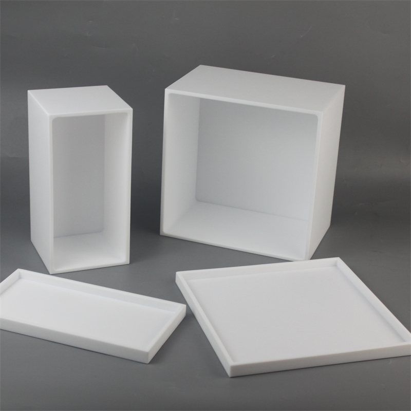
We understand that wafer handling processes vary significantly across different laboratories and production lines.
This PTFE wafer box can be fully customized to match your specific wafer processing workflow, including:
From single-wafer storage to complete wafer processing container systems, we provide tailored PTFE solutions to ensure compatibility, efficiency, and contamination control throughout your workflow.
FAQ
Q: What's the lead time for orders?
A: Standard models ship in 7 working days; customized units require 15 working days or more(Depending on the level of complexity) after payment.
Q: Can I request a customized size?
A: Absolutely! We offer tailored attachments.
Q: How do you handle shipping and delivery?
A: We deliver goods efficiently via express services such as DHL, FedEx, and UPS, as well as various other methods including air and sea freight.
Q: How do I place an order?
A: Contact us via email or leaving a message for a quote, then confirm with a PO.
Leave A Message